Difference between revisions of "TDT RZ6"
Jump to navigation
Jump to search
| Line 4: | Line 4: | ||
===Digital I/O=== | ===Digital I/O=== | ||
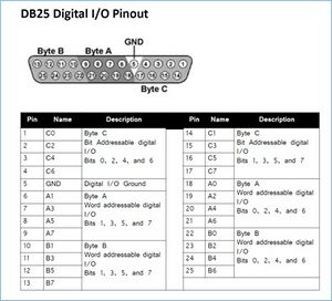
| − | [[File: RZ6_DB25_Digital_IO_pinout.jpg|thumb|DB25 Digital | + | [[File: RZ6_DB25_Digital_IO_pinout.jpg|thumb|DB25 Digital I/O pinout]] |
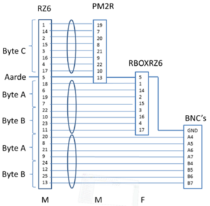
| + | [[File: PP_RZ6_Digital_IO_connections.png|thumb|PP RZ6 Digital I/O pinout]] | ||
Figure 1 shows the pinout scheme of the digital I/O of the RZ6, in the lower left corner of Figure 6. Figure 13 and Figure 2 give the connection scheme of the RZ6 to the multiplexers, response box and Refa. See also Figure 10. PP refers to: “Patch Panel”, a switchboard with connectors. | Figure 1 shows the pinout scheme of the digital I/O of the RZ6, in the lower left corner of Figure 6. Figure 13 and Figure 2 give the connection scheme of the RZ6 to the multiplexers, response box and Refa. See also Figure 10. PP refers to: “Patch Panel”, a switchboard with connectors. | ||
Revision as of 14:21, 8 January 2024
Description
%todo
Digital I/O
Figure 1 shows the pinout scheme of the digital I/O of the RZ6, in the lower left corner of Figure 6. Figure 13 and Figure 2 give the connection scheme of the RZ6 to the multiplexers, response box and Refa. See also Figure 10. PP refers to: “Patch Panel”, a switchboard with connectors.


